Default settings
One of the annoying thing with this 'SPECIAL' edition of the firmware are the default settings:
- Frequency Offset -160MHz
- Resolution 5 digits
One of my goals while disassembling the formware was to 'fix' these defaults settings. I was wondering wether they where located in an undocumented part of the EEPROM or directly as hardcoded values in the firmware itself.
I have partially understood the setup routine, the one called from the RST vector; the interrupt vector is located at addresses 0xFFF2-0xFFFF, with the RST routine address being at 0xFFFE. In my case, the RST handler is located at 0x5F19:
FFF2 svec_SWI3   FDB     hdlr_SWI3                ;08 20
FFF4 svec_SWI2   FDB     hdlr_SWI2                ;9E 90
FFF6 svec_FIRQ   FDB     hdlr_FIRQ                ;48 45
FFF8 svec_IRQ    FDB     hdlr_IRQ                 ;70 F1
FFFA svec_SWI    FDB     hdlr_NMI                 ;00 00
FFFC svec_NMI    FDB     hdlr_NMI                 ;00 00
FFFE svec_RST    FDB     hdlr_RST                 ;5F 19
But completely disassembling the whole RST routine is slow and difficult. At some point, I found that a smarter approach would be to compare the content of the RAM after a fresh start and after having modified some configuration values, like the Frequency Offset.
The RAM addresses where the offset values are documented in the Service Manual, unfortunately, each model as its how address map, and no available Service Manual covers the EIP 545B. So I first needed to find where the frequency offset is stored in RAM so I can then look where this area is modified in the firmware.
Thanks to the TEST10 allowing to read any address in the address space (be it RAM, EEPROM, EPROM or even I/O registers), I wrote a simple Python script to read the whole content of the RAM via GPIB.
It's very slow, since I did not find a way using GPIB commands to read 2 memory addresses without quitting the TEST10 mode between two reads. And I had to add several sleep() since the EIP is pretty slow to respond to GPIB commands. A complete dump of the 2ko RAM took somethin like 15 or 20 minutes.
I did not even wrote a script, in fact, just throw some code in an IPython session. However, the crude code looks like:
import serial
cnx = serial('/dev/ttyUSB0', baudrate='115200')
cnx.write('++addr 17\r\n')

def rd(x):
    cnx.write('TA10\r\n')
    time.sleep(0.1)
    cnx.write('%04X\r\n' % x)
    time.sleep(0.1)
    cnx.write('++read\r\n')
    time.sleep(0.05)
    r = cnx.read_all()
    cnx.write('TP\r\n')
    return r

def getmem(n=0x800):
    out = []
    for x in range(n):
        v = rd(x).strip()
        v = v.split('-')
        out.append(v)
        time.sleep(0.5)
    return out

ramcontent = getmem()
# [...] write ramcontent in a file
This allowed me to quickly find where the Frequency Offset is stored: 0x0276-0x027C (using the format described in the service manual).
For the number of digits, I'm not sure yet, but it looks to be located at 0x0045 or 0x0046.
So I could then look for this Freq. Offset address (OxO276) in the firmware: It's used directly only a couple of times in the code, one of them lloking like:
6118             LDX     #M0276                   ;8E 02 76
611B             LDA     #$01                     ;86 01
611D             STA     ,X                       ;A7 84
611F             STA     $02,X                    ;A7 02
6121             LDA     #$60                     ;86 60
6123             STA     $03,X                    ;A7 03
in which we can see that the value 0x01 (from register A) is stored at address 0x0276 and 0x278 (thanks to the STA $02,X instruction, with X being 0x0276 when this former instruction is executed, it stores the content of A (0x01) at addres 0x0276+2=0x278), and the value 0x60 is stored at 0x0279 (STA $03,X).
It worth noting that this snip of code is executed shortly after intializing the RAM content to zero.
So the result of this piece of code is that the content of the RAM at this 0x0276 address is:
01 00 01 60 00 00 00
ie., conververted in frequency: -160MHz, the initial value I want get rid of!.
So I just have to replace these code by NOP instructions and it should be fine for the Frequency Offset, which I haven't done yet (I was waiting for a cheap EPROM eraser from eb, which just arrived).
Concerning the resolution, some clue can be found just after the previous routine:
6125             LDX     #M005D                   ;8E 00 5D
6128             LDA     #$0D                     ;86 0D
612A             STA     $01,X                    ;A7 01
612C             LDA     #$05                     ;86 05
612E             STA     >M0045                   ;B7 00 45
In which the value 0x0D is written at RAM address 0x005E (0x005D + 0x01 from the opcode STA $01,X), and the value 0x05 is written at RAM address 0x0045, which we identified previously as a candidate for the digits resolution setting; pretty consistant with the 0x05 value written there. Not sure what the 0x0D is used for at address 0x005E.
The sensitivity problem
I have also investigated a bit the sensitivity problem I have on band 3: I can hardly detect signals lower than -10dBm at 1 or 2GHz, where it should be able to catch a -30dBm.
I've tried to recalibrate (on that frequency range) the YIG filter, it did not help.
Following the advise of HighPrecision on the eevblog forum, I did give a check at the SMD capacitors in the IF amplifier/detector detector part of A201. I still need to investigate more, but I haven't found an obvious culprit in there.
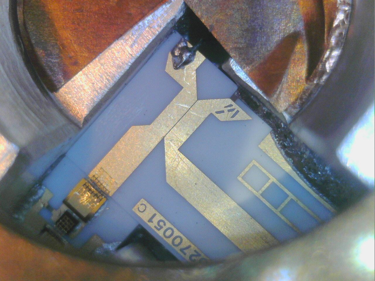
But since I had disassembled the A203 unit, I also gave a closer look at the YIG filter itself, taking pictures with my small USB microscope.
On one side is the ceramic support for connections from the output YIG coupling loop:
On the bottom side, we can see the YIG spheres and the coupling loops:
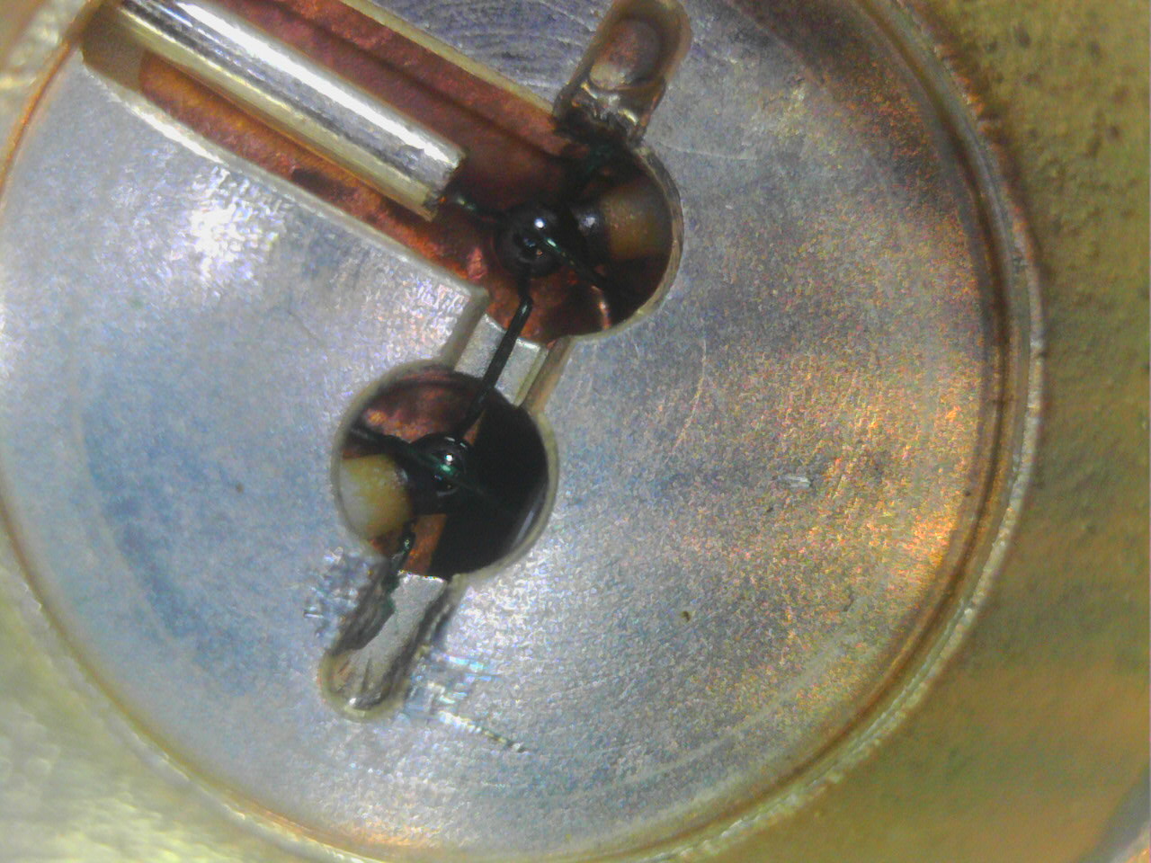
So this filter consists in a 2 stage bandpass filter (with input and output couplig loops at 90° each other).
Having a closer look, the problem appears:
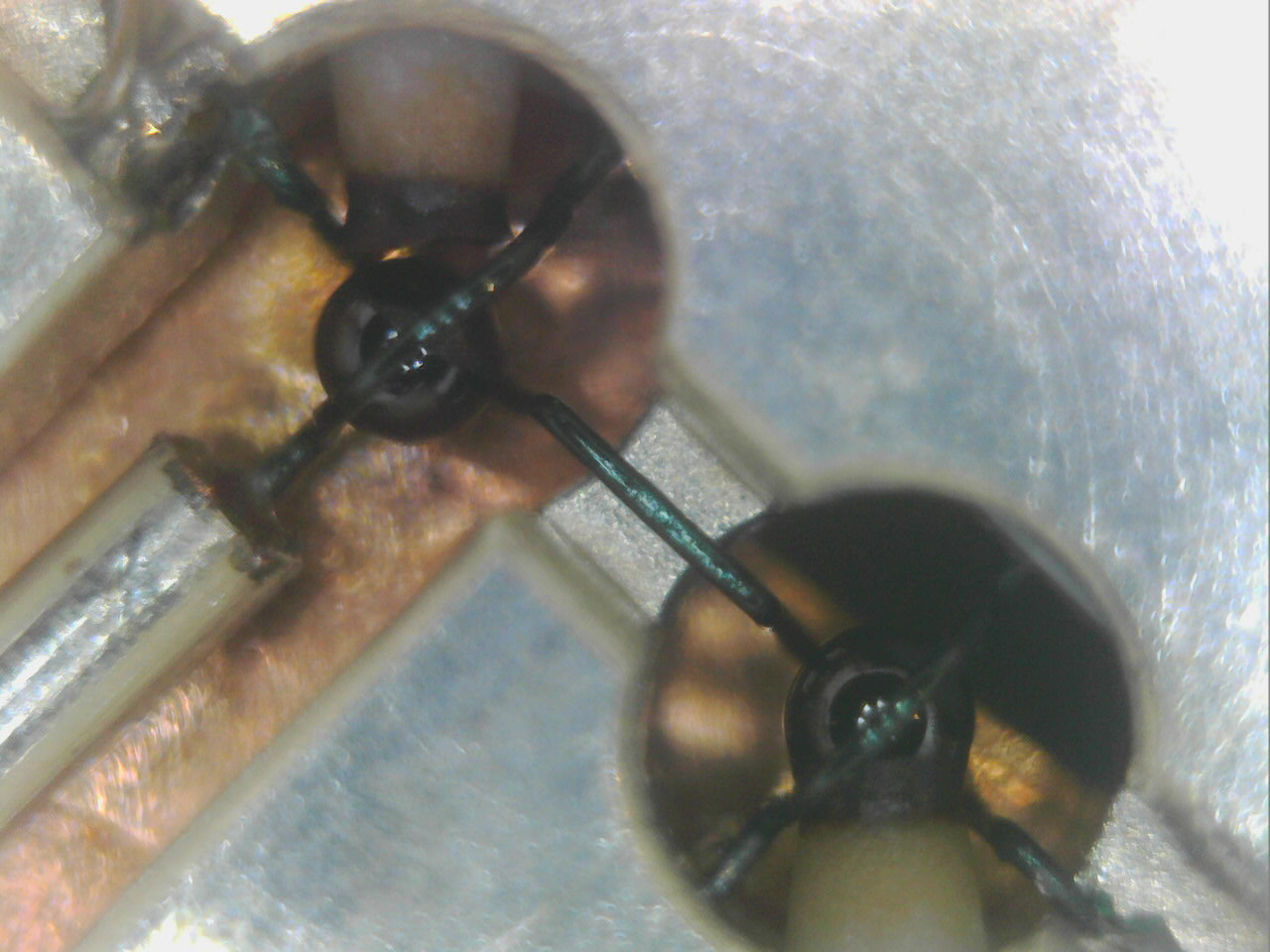
As can been seen there, the YIG sphere took off the holding rod. Tha cage made of the 2 coupling loops is small enough the sphere stayed there, but it is not at the center of the 2 loops any more, nor it is correctly orientated. No surprise the input signal is so low (in fact the suprise is that is still works somehow).
I tried to move the sphere a bit, using a sharp (as sharp as possible) wooden stick under the USB microscope, but it is really hard to orientate the sphere (which diameter is around 0.1 or 0.2mm).
I'll try again, just in case, since I can see the mark of the rod on the sphere, I think I may be able to roughly reorientate the sphere, but it is really hard to do without micrometric actuators.
Meanwhile, I've bought on eb a cheap (20$) A203 assembly. It's not exactly the same model (it's probably one for the 26.5GHz version, according to HighPrecision), we'll see if it works. I hope it's a 127MHz version, otherwise I'll have to replace the YIG filter (A201) on my A203 unit with this one.
By the way, for thoses interested, I found these 2 simple documents interesting to begin to understand how a YIG oscillator and a YIG filter works: