Band 3 Sensitivity
I have been trying to figure out a bit more about the sensitivity problem described in part 3.
The main problem remains the first YIG sphere that has fall off the holding rod. I have tried to manipulate it with thin wood stick, under my cheap USB microscope, but as expected, this operation is very difficult.
So for now, this is not fixed at all.
However, I was wondering if this YIG sphere was the only problem involved in this lack of sensitiy.
As far as I can understand how the unit works, there are 2 level-related output signals from the A203 assembly: the Band 3 RF level signal and the IF threshold signal.
The overall process of the Band 3 is as follow:
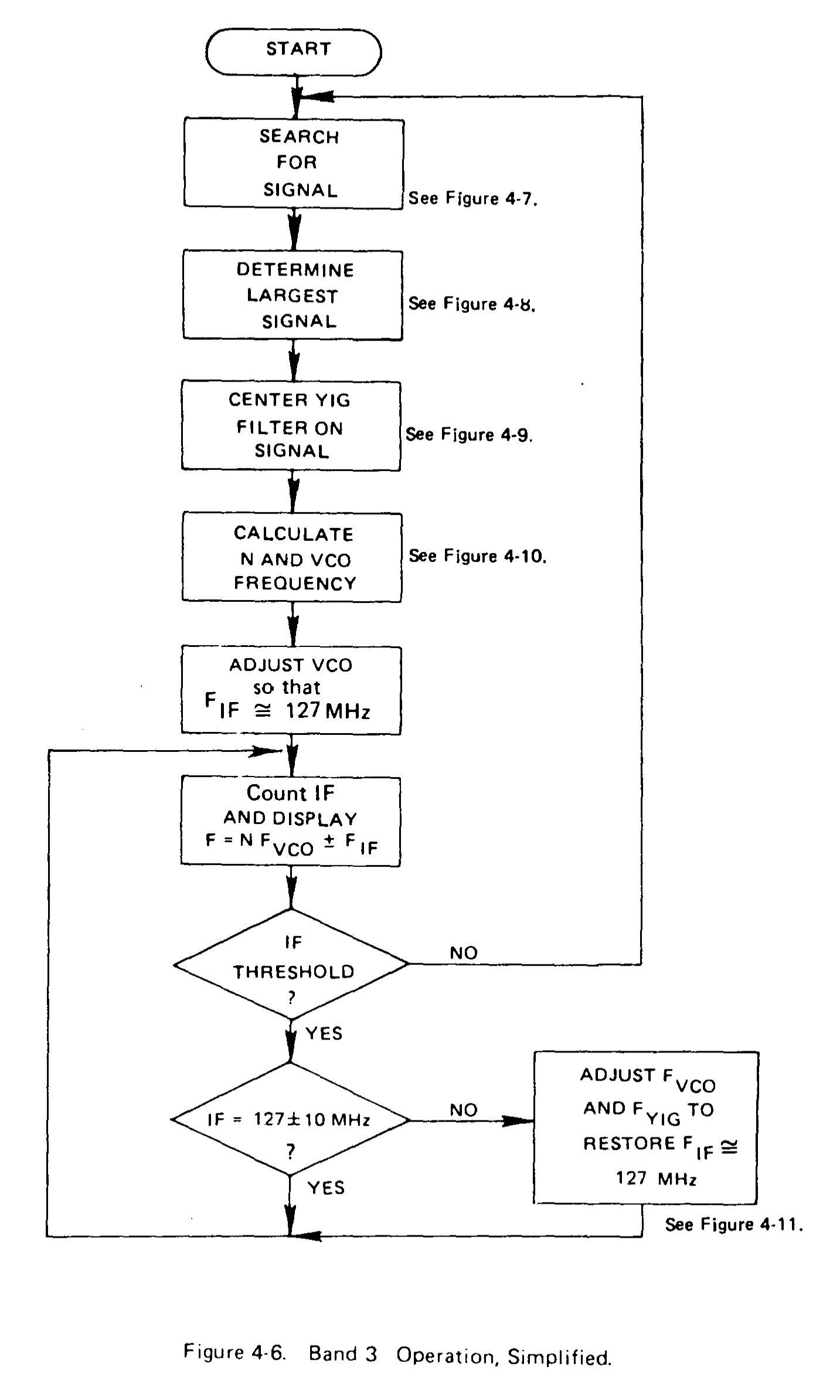
For which the first step is the search for signal:
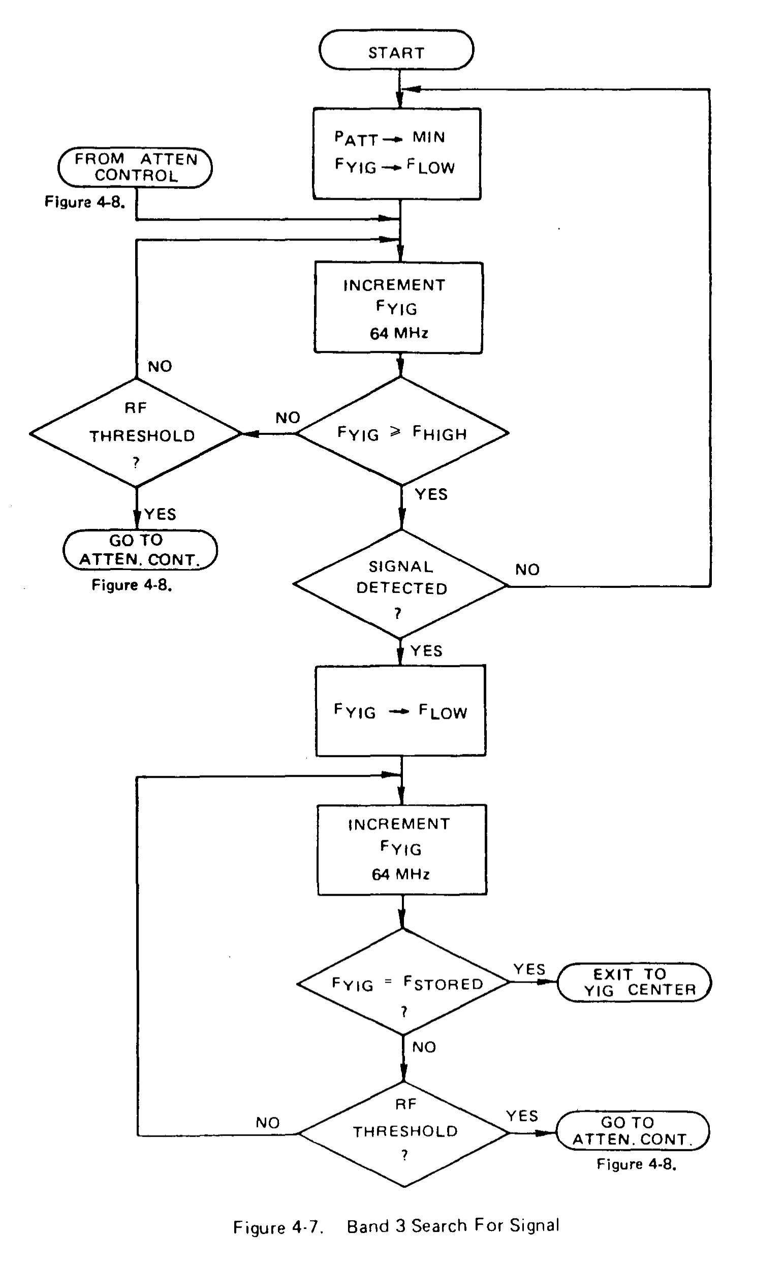
I seems to me that the RF level is used for two purposes: in the search for signal operation first, to measure the RF level then.
The RF level is measured from the so called "Video Amplifier", which can has a gain of around one, or can be set to +15dB.
So another possible culprit could be the this section of the Video Amplifier.
Unfortunately, the schematics of the A203 assembly is not available in the service manual:
The assembly drawing and schematic for both the VCO and IF circuits are not available. The entire A203 assembly must be tested as a complete unit to ensure proper performance of the counter. Repair of the Microwave (YIG) module can only be done at the factory. The VCO and IF Amplifier boards require special test equipment, therefore field repair is not recommended.
RF and video amplifier
In order to understand, I have drawn the schematics of the board on which are the IF amplifier and the video amplifier:
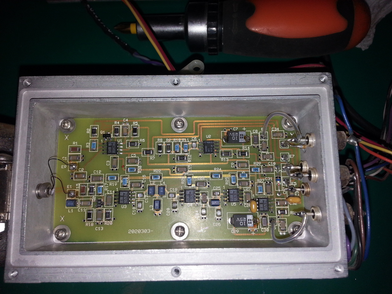
Fortunately, the board is quite simple, and despite being made of SMD components, single sided.
The schematics looks like:
The video amplifier consist of a simple MC1458 opamp (mainly a dual 741).
The 15dB gain is selected by an input pin, leveled by the first half of the MC1458 (used as a comparator) driving of transistor. The marking on the SOT-3 package is 6A Y, which is not easy to find. I finally figured it might be 2SJ106, a JFET transistor.
Before finding the kind of transistor it is, I though it was faulty, because a simple measurement of the DS with an ohmmeter gives a low value (around 200 ohms). It took me a little while to rememeber it's a normal behaviour for this kind of transistor (the Drain and the Source being two sides of a single piece of silicon).
I removed it from the board, but a quick check using a 20$ LCR/transistor meter showed it looks fine.
However, I also need to have a rough understanding of the YIG filter and mixer assembly.
YIG filter filter and mixer assembly
The YIG tuned filter and mixer assembly looks like:
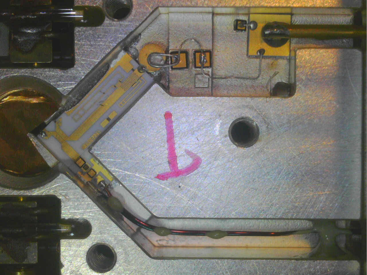
Once again, I am trying to understand what this whole thing works, but I really don't have the knowledge to do so, really.
Looking at this macro photo of the output stage of the YIG filter, it looks like a single diode balanced mixer. The LO signal, provided by the VCO, is coupled with the input signal comig from the YIG filter.
It looks to me that the first square block after the coupler could be a mixer diode (otherwise I really don't understand how this could act as a mixer).