After a loooong pause on this project, I have recently been able to work on it again. In the previous post in this series, I've started to implement a replacement board prototype based on a an NUCLEO board and an SSD1322-based OLED display.
Meanwhile, I have also almost completely described the communication protocol between the main unit and the front panel.
In this episode, I'll describe the next steps: make the circuit diagram and the PCB for the replacement board.
Circuit diagram
The circuit diagram is rather simple:
- an STM32 MCU (I initially chose the STM32F303RE, but finally used an STM32F303RD just because the former was out of stock when I made my command at mouser.) I wanted an STM32 MCU with USB support and reasonnable amount of flash and ram just not to have to worry about these while writing the firmware.
- a 8MHz crystal so the clock config used on NUCLEO boards can be used as is.
- a step-down DC-DC converter to go from the +18V coming from the main unit to +5V to power the OLED display and the some chips on the board; I've chosen a TPS560430 from TI,
- a 5V->3.3V LDO regulator to power the MCU, an MCP1811AT-033 by Microship,
- a level shifter for the communication lines bertween the MCU and the main unit (5V vs. 3.3V logic). For this, instead of going through individual Mosfet transistors, I've chosen the LSF0204PWR from TI, to simplify a bit the assembly (this chip really is not much more than a bunch of transistors in a TSOP package).
Here is the diagram I ended up with:
PCB design
I've used librecad to draw the edge profile of the PCB, after having carefully measured the broken PCB, and a kicad plugin to generate nice keypad footprints. (I had to adjust the generated footprint by hand to make it more usable.)
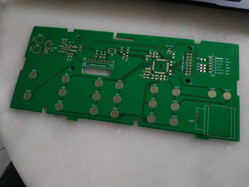
The end result looks like:
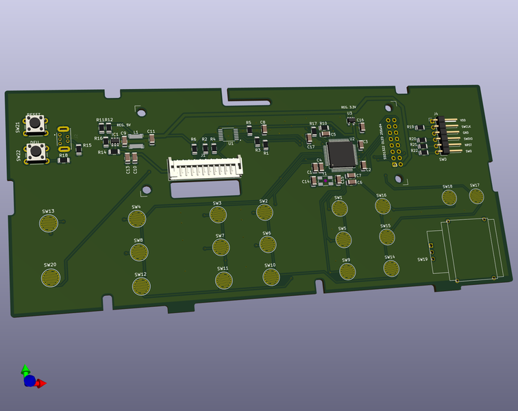
The 2 buttons on the left are the Reset and the DFU boot mode. The header on the right is the SWD port.
After a few days, the PCB arrived (from the usual places):
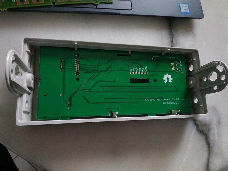
And it fits just fine in the front panel enclosure:
Unfortunately, I made a few mistakes in this design (see below) bit I also made the big mistake of swaping the marking of R11 and R12, which defined the feedback divider setting the output voltage of the DC-DC converter. As a result, I fried a LDO and a STM32F303RD chips!
But once replaced correctly, is began to work:
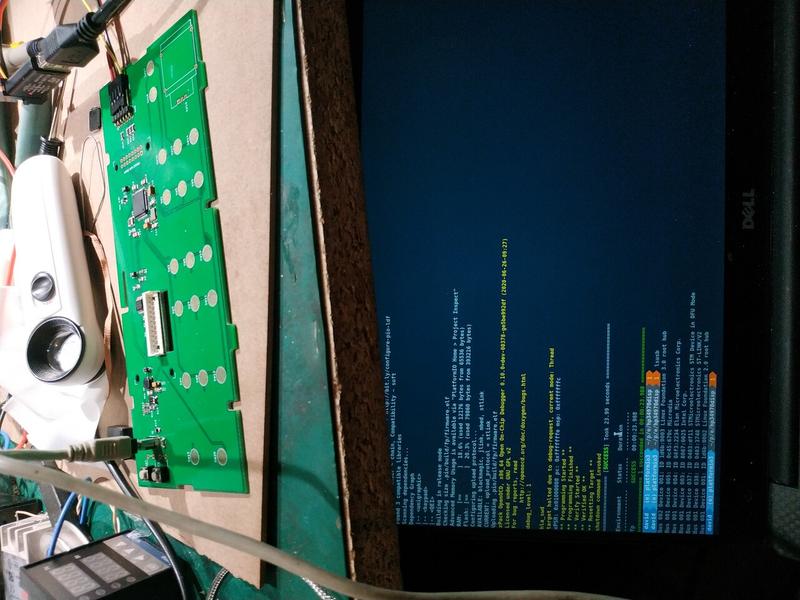
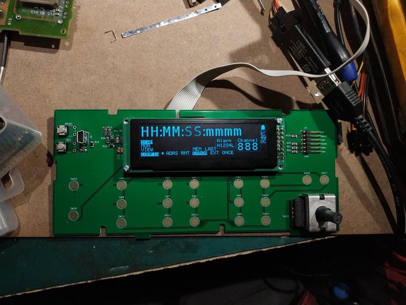
After installing the OLED display and adjusting the previous verison of the code (which was designed for the NUCLEO F446RE board), I could compile it for my custom board and make it run:
Firmware design
At this point, I tried to make the CDC USB driver work on the board, but I failed to do so. I realized that the USB stack is actually missing for this MCU in MBed OS 6. (update: there is a PR waiting to be accepted and merged to improve support for the STM32F303 family).
Unfortunately, I could not make the debug pin of the SWD port work either. I can upload a new firmware juste fine via this SWD port (in addition to the DFU mode via USB), but I have been ablt tuse the SWO ping to get a console to see print statements.
In last resort, I ended up soledring thin enameled wired directly on the MCU's pin to get access to of the available UARTs as console/debugger.
At least this worked just fine, and I could then work on the code much more easily.
I also had to use my DSLogic logic analyzer to debug a few things and get to a point that make the front panel usable:
In this version of the code are many remaining problems, the biggest one being the fact the display flickers a lot. In the code of the formware, I have a "frame"-buffer in which the main loop draw the information to be displayed, and a thread that copy this buffer to the actual display once every 30ms. And in the first version display above, there was no DMA involved in tranferring the buffer into the display unit.
Activating the DMA did help a bit, but was not enough to get rid of the glitches. The real problem was there was no lock around that buffer, so the display refresher thread was making the transfer at any time, including in the middle of the drawing proceure. Adding a lock around this buffer finally fixed the problem.
Another problem I had in the first version of the firmware was the fact a keypress event could be sent to the main unit during a transmission of a packet by this later, which mess the transmission protocol quite a bit. This problem is now (mostly, not 100% sure there is no edge case left) fixed.
Here is an example of this situation occuring (screenshot of a PulseView session):
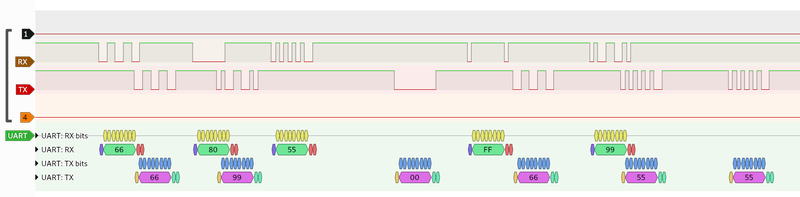
In the example above, one can see the front panel is starting a transmission (sends a 0x66 on the RX line), but while this byte is being sent, the 0x66 start of transmission byte is also sent by the main unit.
Not sure yet how to fix this, either by making sure that this situation does not occur (which is most unlikely not feasible), or by impriving the transmission protocol handling state machine in my firmware to be aware that this may happen and be resilient against it.
But in the end, I've now reach a point where the firmware begins to be really usable:
Design errors
Making this circuit I made a few mistakes and errors.
Wrong MCU
I've not paid enough attention when I chose the MCU. The STM32F303RE I chose is more then fine on a specifications point of view, however, since I am writing the formware using MBedOS, I did pay attention that the USB FS stack is not yet supported for this MCU on MBed OS 6.
My initial idea was to provide a serial communication protocol with the front panel to be able to upgrade the firmware easily or get the current display content, but this is for now not possible. Will have to stick to GPIB for now.
No proper USB VBUS handling
I decided not to connect the VBUS power line from the USB socket, but it would have made my life a bit easier to connect it via the usual protection, so the testing / uploading the firmware could have been a bit easier until the front panel wasa plugged back to the main unit.
Even so, it would be nice to be able to upgrade the firmware without having to plug the whole unit.
The real problem of not having connected the VBUS signal is USB detection. If I want to be able to implement a USB connection, I need to be able to detect wether the USB connector is plugged, and the simplest way of doing that is to detect the presence of the VBUS signal.
No diagnostic/status LED
I should have added a few diagnostic/status LEDs: there are plenty of GPIO left unused on the MCU, having those visble indocators is alway handy.
No extra UART
I should have routed at least one unused UART from the MCU to a pair of headers: it way easier not to populate such a header than to hack small wires directly on the MCU tget a decent console port...