This is the part 2 of the series about my HP 3562A Digital Signal Analyzer, quickly describing the Digital Section of the instrument.
Digital Section
The unit is quite capable, since the main CPU is a 68000 (not exactly of small CPU for the time).
The 8 boards are:
- A1: Digital source and front-end interface (rev B, ref: 03562-66501)
- A2: CPU & GPIB controller (rev D, ref: 03562-66502)
- A3: Memory (rev B, ref: 03562-66538)
- A4: Local oscillator (rev C, ref: 03562-66504)
- A5: Digital filter (rev B, ref: 03562-66505)
- A6: Digital filter controller (rev D, ref: 03562-66506)
- A7: Floating Point Processor (FPP) (rev B, ref: 03562-66507)
- A9: FFT (rev B, ref: 03562-66509)
The service manual also describes an A8 board with additional RAM, but my device does not have such a board. It looks to me that my version of the DSA has both extra ROM and RAM on the A3 memory board.
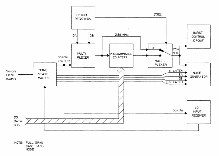
Digital Source
Note
The Service Manual available on the net lacks a few pages in the Digital Source section, so I do not have details on the Timing Control section.
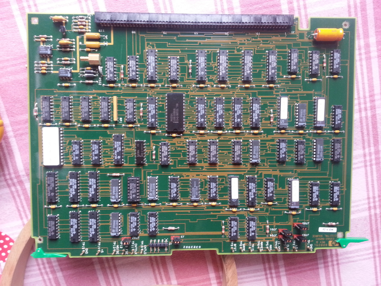
This board is mainly responsible for generating the digital signals that are used as input for the source DAC. It generates all sort of noise figures, bursts, sweeps, and so on.
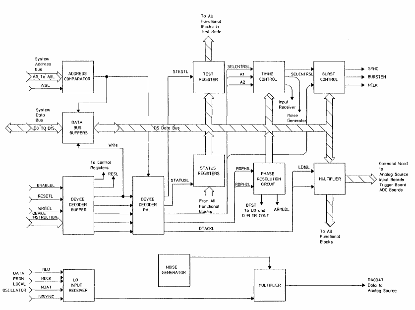
The Timing Control section looks like:
The Phase Resolution is used in external and internal triggered measurements, ensuring that the phase of a triggered measurement is accurate. Since the trigger moment does not always occur on a sample and hold edge, there is a time delay and phase error in the data. This phase resolution circuit counts the time between the samples and a trigger.
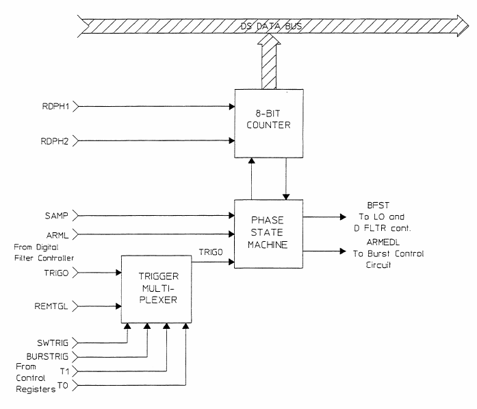
The Burst Control circuit controls the burst length and generates the pulse signal to the Local Oscillator (A4). It provides the gating signal that gates the analog source on and off during the burst and chirp modes.
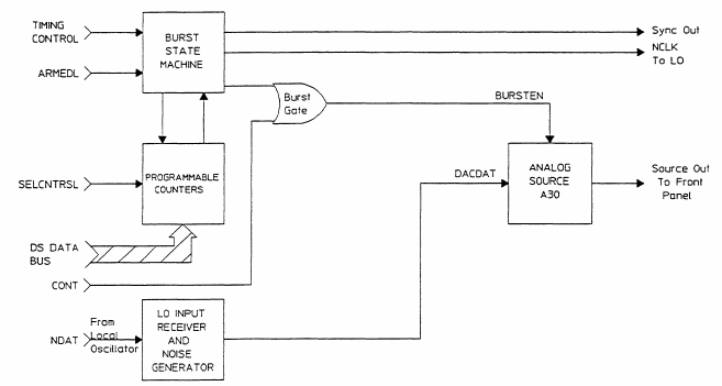
Other parts of this board are the LO Input Receiver that synchronizes the local oscillator input data to the sample rate, the Multiplier that multiply the LO data by the noise and send it to the analog source, and the Noise Generator that produces binary random sequences that is used for band-limited random noise and burst noise signals.
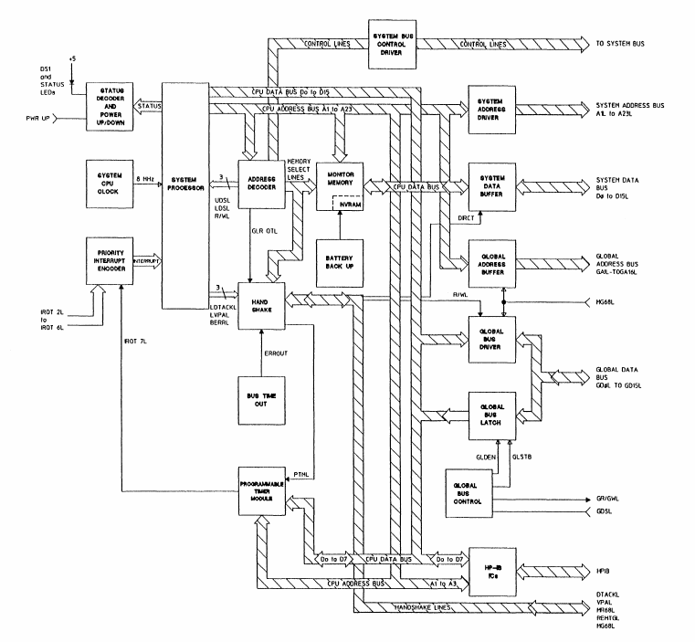
CPU
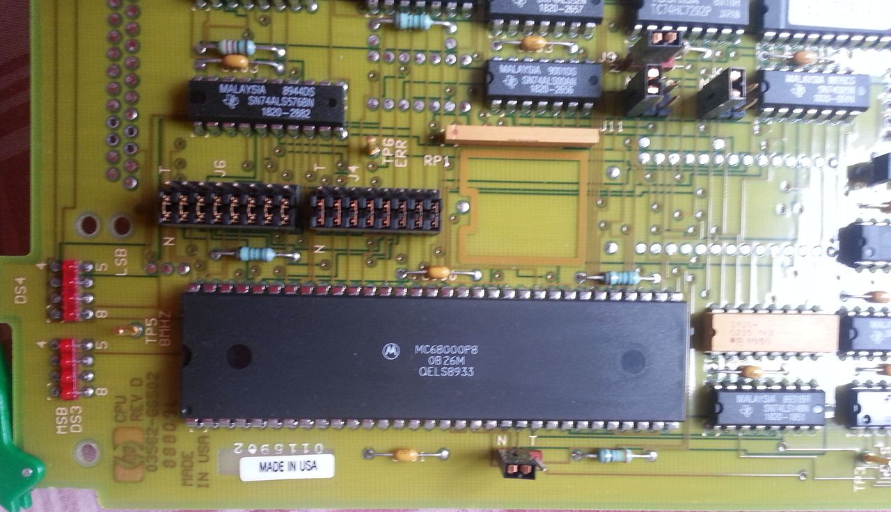
The processing unit is a MC68000. It aims at telling each assembly which process to execute and monitor the overall functionning and data processing of the instrument.
The main CPU board, with the beautiful MC68000P9 DIP64 package:
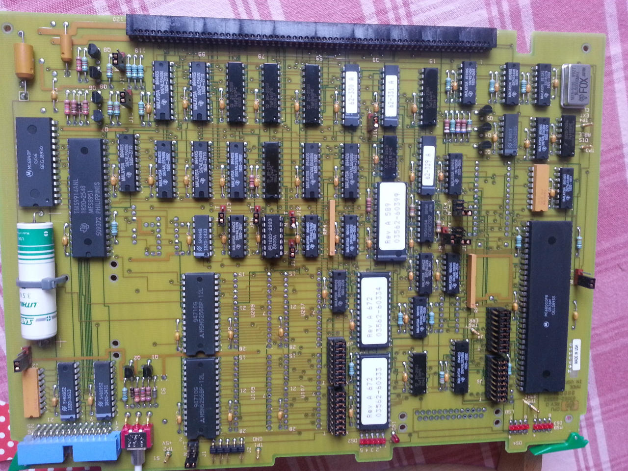
It comes with 2 populated M5M256BP static ram chips (32k x 8bits), for the CPU, but seems to be capable of holding 4 more of them. The CPU runs at 8MHz.
There is also some ROM, the main "boot loader" program. Unfortunately, neither of the ROM chips are mounted on sockets but are directly soldered on the PCBs, so I did not took the risk of damaging one of them by desoldering them for dumping their content.
Most of the remaining of the circuit is to manage the global data bus, the system bus, the IRQs and the GPIB bus.
The blue connector is for the GPIB connector.
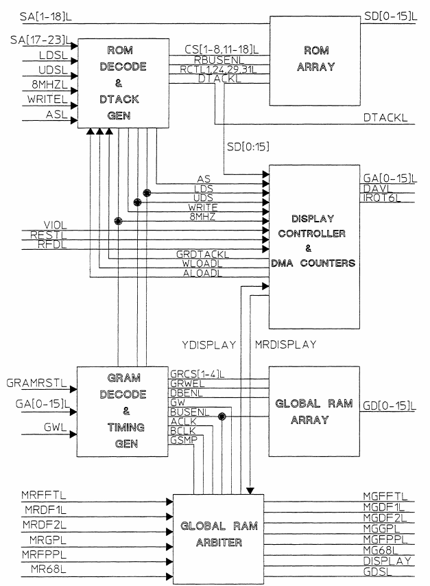
Memory
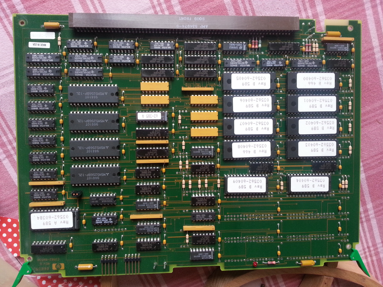
This board is described as an "extension of the read only memory of the system CPU board" and read/write memory used by most of the other assemblies.
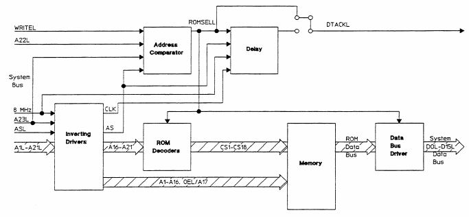
The ROM section stores most programs for the HP 3562A except the startup routines (which are on the ROM ships of the A2 CPU bloard).
The board allows flexibility in the number and type of ROM chipes used. ROM density is selected by placement of jumpers.
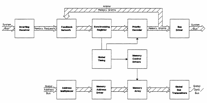
The RAM section of the assembly consist of 4 32k by 8 bits static RAM chips as well as the arbitrer section which controls access requests to the global RAM from six devices (FFT, both Digital Filters, Display, FPP and the system CPU).
The Display Controller section also lies on this A38 board.
Note
On older versions of the instruments, this board was splitted in 2 (A3 and A8) and used less dense chips (thus, much more chips).
Local Oscillator
The Local Oscillator produces digital sin and cosine signals (synchronized with the sample rate). The sinusoidal signal is generated from a table of values stored in the ROM.
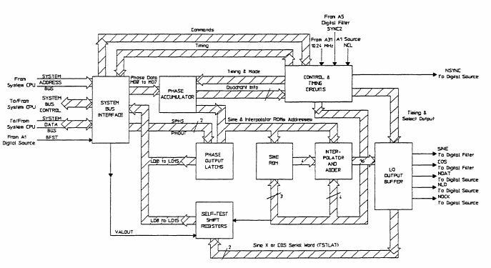
Block diagram of the A4 local oscillator board of the HP3562A
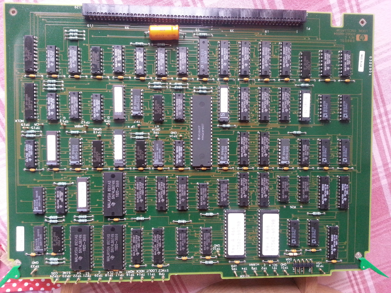
Picture of the A4 bloard of the HP3562A
Digital Filter and Digital Filter Controller
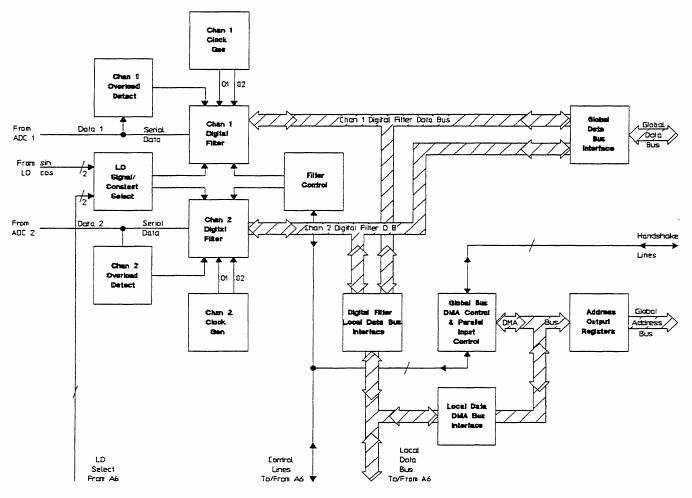
The Digital Filter Assembly consists in both A5 and A6. It processes two channels of serial data coming from the instrument front end (ADC) ans stores the results in global RAM. Processing consists of conversion from a serial format to a parallel format and, if required, digital filtering or zoom (a combination of frequency shifting and filtering). The processed data is transferred on the global data bus.
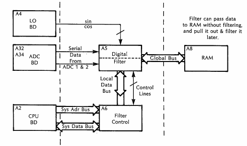
Digital Filter Assembly block diagram.
Digital Filter: Each digital filter consists of a control IC and 2 filter ICs, one for the real data and one for the imaginary data.
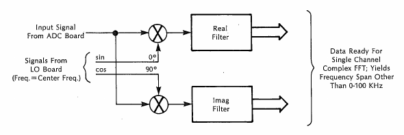
The Digital Filters are fed with a kind of LF I/Q demodulator, used for zooming or actual digital filtering.
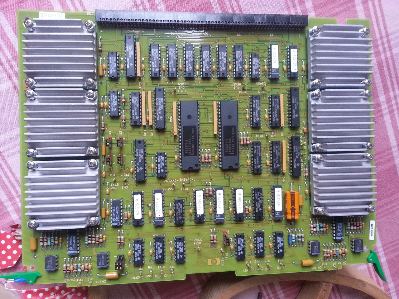
Picture of the A5 Digital Filter board.
The A5 Digital Filter board block diagram.
Clock Generator: The clock generator creates two complementary clock pulses from the 10.24MHz system clock.
Overload Detect: The first 3 bits in the ADC serial data stream contain overrange information that must be stripped off the serial data.
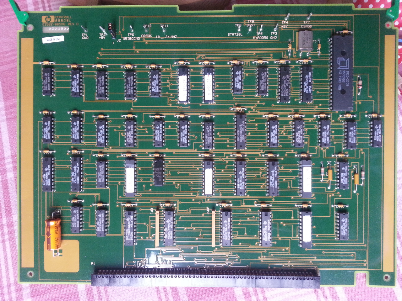
Picture of the A6 Digital Filter Control board.
The A6 Digital Filter Controller board block diagram.
FPP
The Floating Point Processor board is a fast arithmetic unit which carries out real and complex arithmetic operations on blocks of data stored in the global RAM. The processing ALUs are six AM2903 bit-slice microprocessor ICs and one AM2910 microprogram controller. Instructions are provided to the ALUs by an address sequencer and seven microcode PROMs.
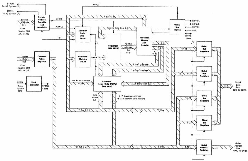
Floating Point Processor block diagram.
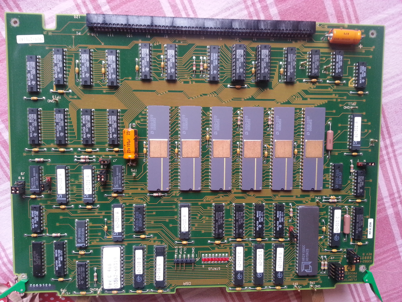
Picture of the A7 FPP board.
This Floating Point Processor is capable of handling 16 bits integers, 32 bits and 64 bits floats.
FFT
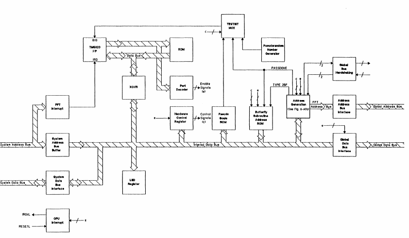
Block diagram of the A9 FFT board
The FFT board performs windowing, FFT and Inverse FFT directly from and to the RAM. It's built around a TMS230 microprocessor runningat 5MHz
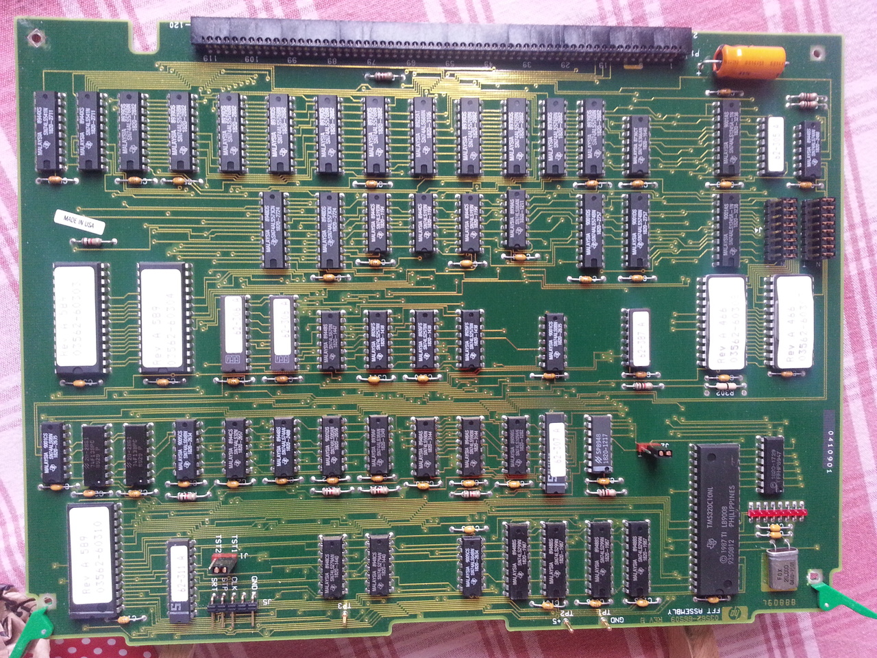
Picture of the A9 FFT board
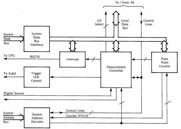
Keyboard
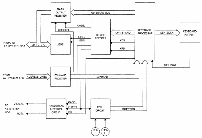
Block diagram of the keyboard processor
Next
In the next part, we will describe the Analog Section of the instrument.