This is the part 3 of the series about my HP 3562A Digital Signal Analyzer, quickly describing the Analog Section of the instrument.
Analog Section
The analog section consist in 6 boards:
- A30: Analog Source
- A31: Trigger
- A32, A34: Input ADCs
- A33, A35: Input
Analog Source
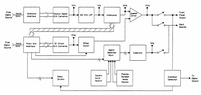
This board is mainly a DAC converting signal signal from the Digital Source board (for sin waves). It also generates Pseudo Random Noise and square waves (used for input calibration).
The analog signal produced by the DAC is filtered by a 100kHz low pass filter, then pass throught a step attenuator (5mV per step). The way this is implemented is quite interesting: the analog signal from the main DAC is used a reference voltage for a multiplying DAC.
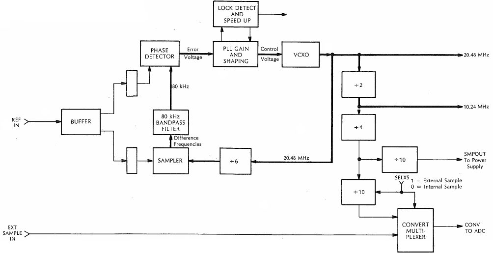
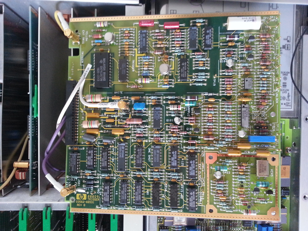
Trigger
A first section of this board produces the trigger signal (for A1 Digital Source and A5 Digital Filter boards) from one of the 4 possible trigger sources: external, channel 1, channel 2 and the calibration.
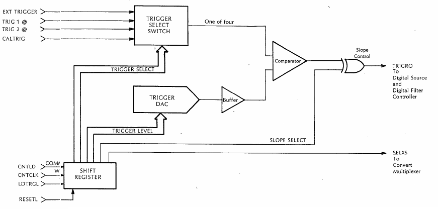
The trigger clock circuit produces the 20.48MHz clock using a VCXO. From this signal are derived the 10.24MHz clock used by many boards (A1, A4, A5, A6, A30, A32 and A34) and the 256kHz clock signal used as internal sample signal.
When an external clock is provided, a PLL is used to lock this 20.48MHz. The external signal can be 1, 2, 5 or the standard 10MHz.
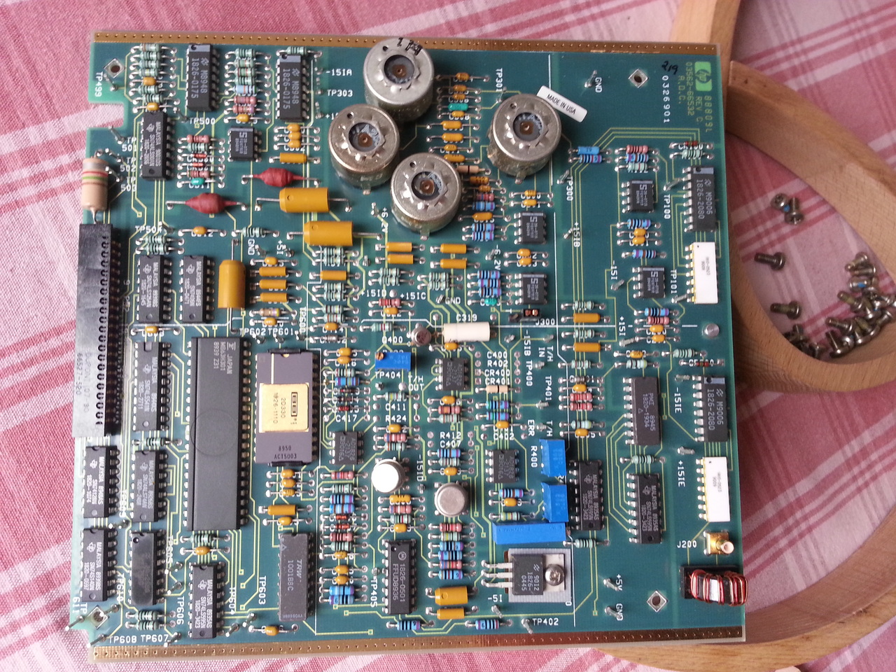
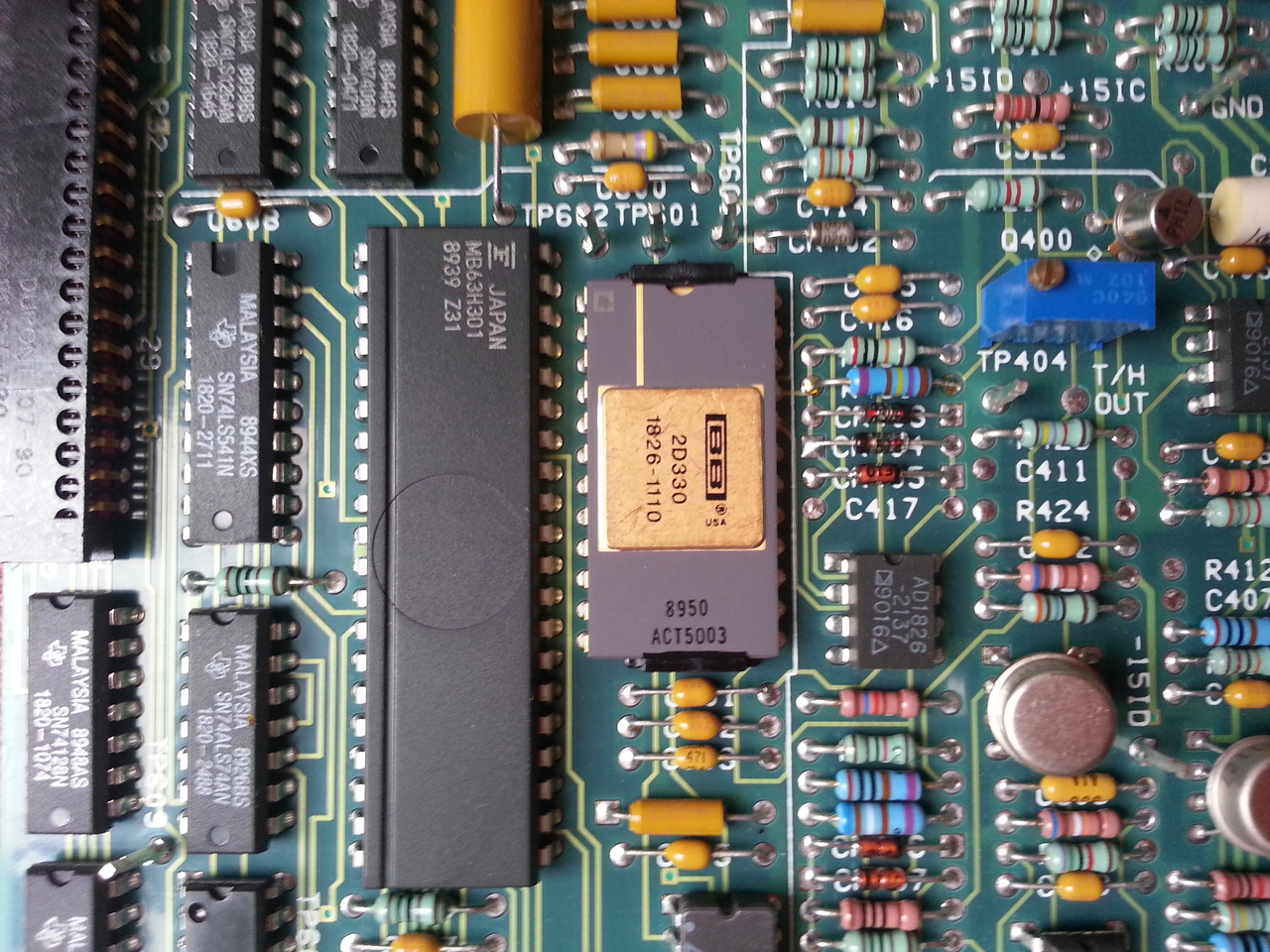
Input ADC
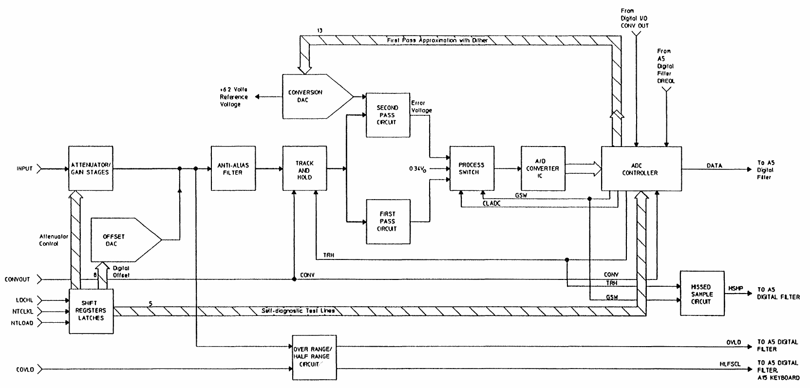
The ADC board converts analog data from the input board into 13-bits serial data words. The Analog to Digital convertion is done in 2 passes by a 8-bits ADC. At each digitilization step, the signal value is frozen by a Track and Hold circuit. This frozen value is digitized (with a 8-bit resolution), then the digitized value is substracted from the input (hold) signal and the result is multiplied then digitized a second time to produce the remaining 5-bits of resolution.
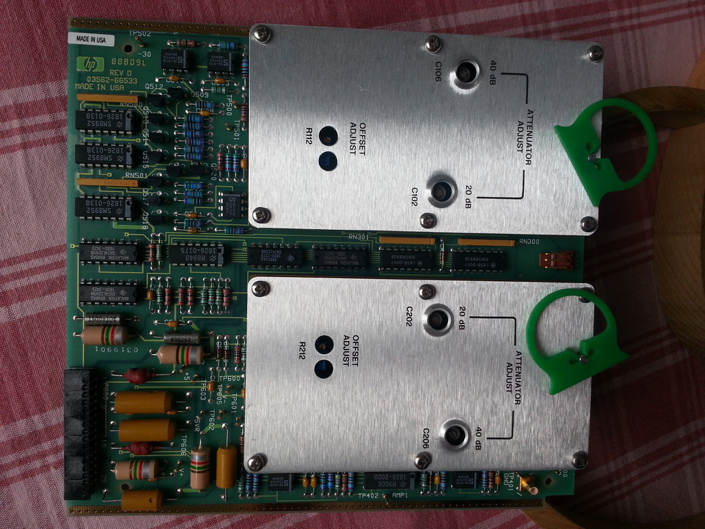
Input
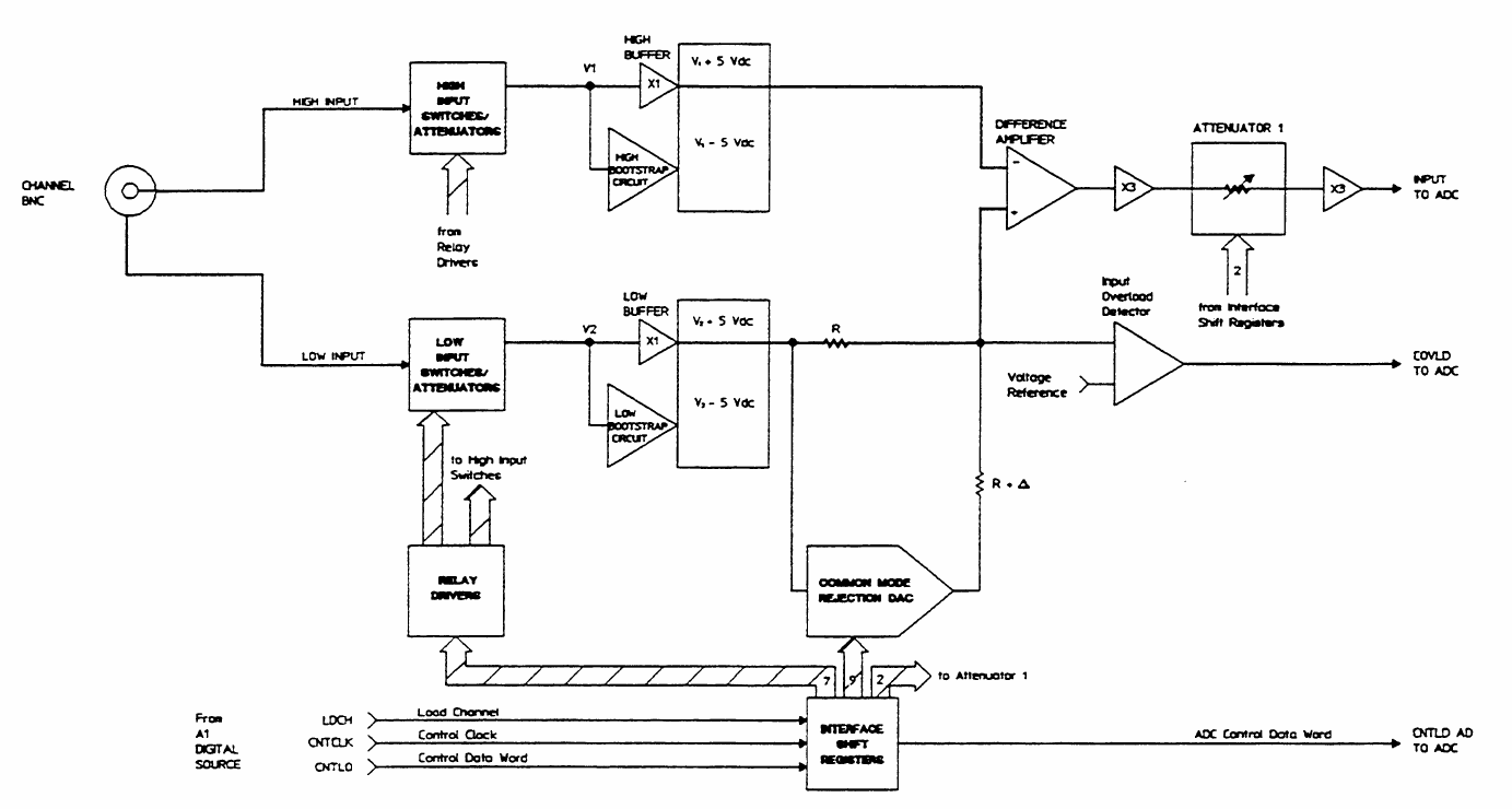
The input assembly implements the voltage ranges and conditions the input signal. It mostly consist in a pair switch attenuators (the input is balanced), followed by a pair of amplifier/signal conditionners. The balanced signal is then fed into a differential amplifier followed by a amplifier and an attenuator.
Next
In the next part, we will describe the HP 1345A Digital Display used in the instrument.