This is the part 3 on my series about my HP 8662A Signal Generator, and is about the third main problems I found with this unit, as evocated in part 2: Error 04 is lit and there are some very unpleasant spectrums at some frequencies.
Low Fequency Section
If the generator is now able to produce a signal (the AM and FM modulations also work), it also gives an Error 04, which is described in the Service Manual as "Sum Loop Unlocked (Low Frequency Section)", and the troubleshooting procedure to follow in on the Service Sheet H. The general block diagram of this section is as follow:
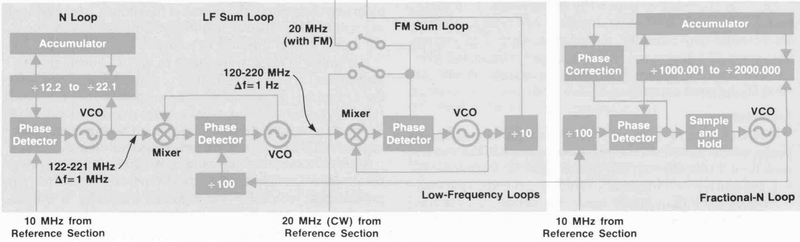
This Low Frequency Section consists in no less than 4 phase locked loops in order to achieve adjustable frequency synthesis with the expected stability and resolution.
In fact, when in the main band of the generator, ie. when neither the output frequency doubler nor the down converter are in the signal path (that is, when the frequency range is between 120MHz and 640MHz). The frequency display consists in 11 digits, named DF0 to DF10, which are segmented to control several sets of PLLs:
|
are the fractional part of the fractional N-Loop (.1Hz, 1Hz and 10Hz digits), | ||
|
are the integer part of the fractional N-loop (100Hz, 1kHz and 10kHz resolutions) | ||
|
are used to set the pretune VCO value for the sum loop VCO (A3A7), the FM sum loop VCO (A3A8) as well as the N-Loop VCO (A3A4). These are the 0.1MHz and 1MHz resolution digits. | ||
|
these control the high frequency section (DF10 can only be 0 or 1, in which case the frequency doubler is used). |
Here is a more detailed vue of the block diagram of the low frequency section:
Fixing the Error 04
The service manual describes the Error 04 as related to the Sum Loop, and the first troubleshooting step is to adjust the LF Sum Loop VCO on A3A7.
To do this, one must open the loop of the PLL to be able to adjust the frequency-to-voltage curve of the VCO.
It took me a while to really understand the service manual on this point, as it explains:
Remove the two jumpers on the A3A7 VCO Assembly a n d plug the board back into its socket.
The problem is that there are no jumpers on that board... In fact, these jumpers exists, but are just soldered wires, and not, as one would expect, jumpers that can be easily unplugged.
Once I finally understood this, I've been able to perform this adjustment. This consists in tweaking two potentiometers to tune both ends of this frequency/voltage curve.
The ideal curve is (all frequencies are in MHz):
| Freq | N-Loop VCO +/- 3MHz | Sum L VCO +/- 3MHz | FM SL VCO +/- .3MHz |
|---|---|---|---|
| 320.0 | 122 | 120 | 10.0 |
| 320.1 | 123 | 121 | 10.1 |
| 320.2 | 124 | 122 | 10.2 |
| 320.4 | 126 | 124 | 10.4 |
| 320.8 | 130 | 128 | 10.8 |
| 321.0 | 132 | 130 | 11 |
| 322.0 | 142 | 140 | 12 |
| 324.0 | 162 | 160 | 14 |
| 328.0 | 202 | 200 | 18 |
| 329.9 | 221 | 219 | 19.9 |
As you can see, ideal curves are pretty linear.
At first, I could not find a correct set of tunings: when I was setting the two ends of the curve to their ideal values (120MHz and 219MHz), the values for 324MHz and 328MHz did not match the +/- 3MHz criterion.
Here is the curve after I adjusted both ends to be as close as possible as their ideal values (the error is inversed to make the plot easier to read; most of the time, I am below the expected value):
As you can see, the +/- 3MHz band is not achieved for most part of the curve. And it looks pretty bad since the max error is above 6MHz. However, I compensated this by overshooting these two points as much as possible in order to try to keep the whole curve within this +/- 3MHz band.
Unfortunately I haven't taken numerical values after this tuning, since this was enough to clear the Error 04.
Other unstable PLLs
After this adjustement, the generator seems to works fine: it does produces a nice output signal (well, I though) and gives no more error. But eventually, playing with the sweep controls, I found some pretty nasty behaviors at some ferquencies.
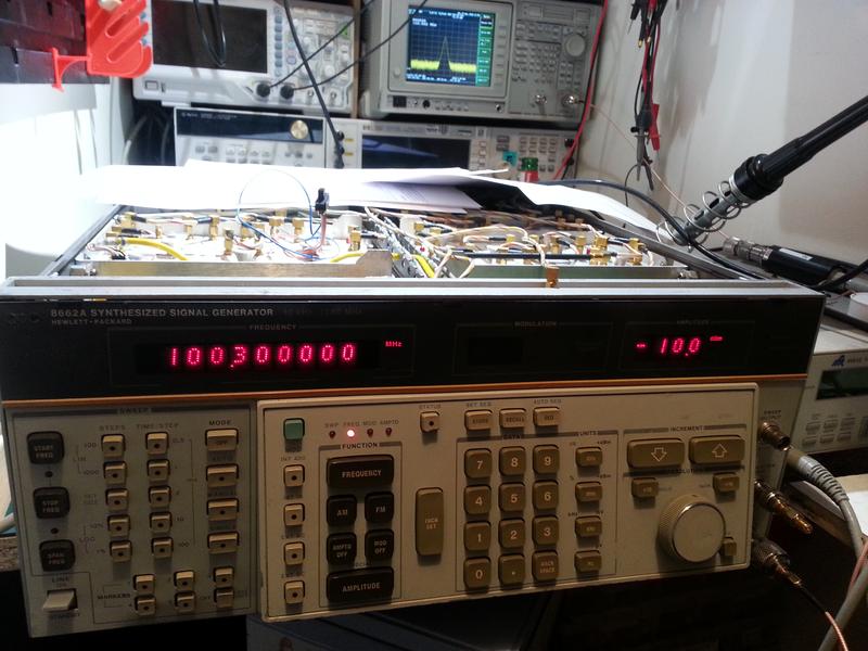
For example, at 100.3MHz, we have a decent signal:
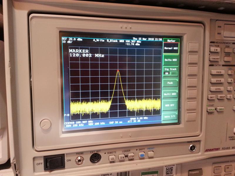
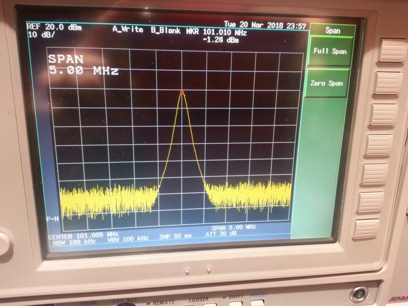
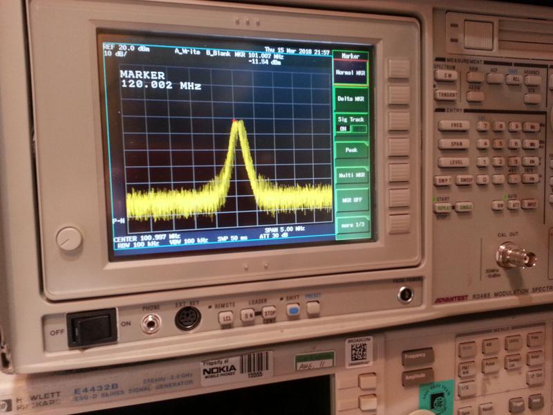
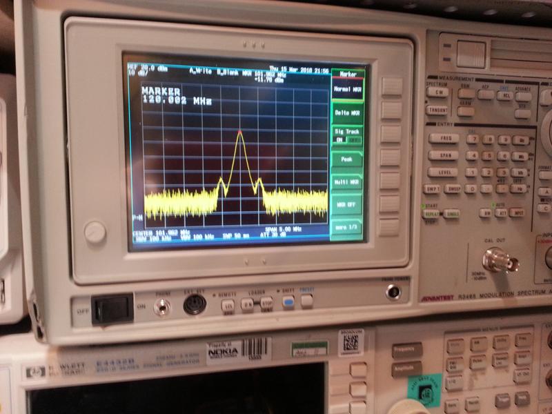
but at 101.0Mhz, it begins to looks pretty messy:
and 101.9Mhz shows "nice" side bands:
The problem seems quite clear: some PLL cannot lock at specific frequencies, but the strange thing is that this unlock PLL does not produces an error.
So I tried to figure out which boad assembly could be the culprit. With no error however, I had to troubleshoot without a procedure.
The funny thing was there was not clear 'pattern' of which frequencies produces the erratic behavior and which worked fine.
The problematic ranges were clearly cyclic upon the frequency range, but the limits were not very stable.
I spent a fait amount of time reading the service manual and reading the schematics to try to understand which board could be the culprit, and measuring value at any testpoint possible...
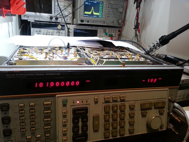
At the end, as I did not make any progress, I decided to try to make all the "post-reapir" adjustments related to the Low Frequency section.
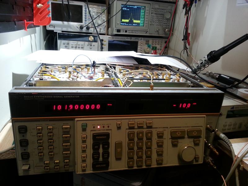
And when I finally tuned the FM Sum Loop VCO, for the procedure is very similar to the Sum Loop VCO one, the problem disappeared.
For example, a 101MHz signal which was very unstable before now looks like: